nanotechnology

Showing posts with label National Institute of Standards and Technology. Show all posts

Nanoscale details of photolithography process

Photolithography Process

Title: Photolithography Process. Description: Schematic of the photolithography process shows the formation of a gradient extending from the photoresist material to be removed (center) into the unexposed portions of the resist on the sides. NIST measurements document the residual swelling fraction caused by the developer that can contribute to roughness in the final developed image.

Source: National Institute of Standards and Technology. Credit Line as it should
appear in print: Credit: NIST. AV Number: 07NCNR002. Date Created: December 2007. Date Entered: 12/11/2007
New paper reveals nanoscale details of photolithography process

Scientists at the National Institute of Standards and Technology (NIST) have made the first direct measurements of the infinitesimal expansion and collapse of thin polymer films used in the manufacture of advanced semiconductor devices. It’s a matter of only a couple of nanometers, but it can be enough to affect the performance of next-generation chip manufacturing. The NIST measurements, detailed in a new paper,* offer a new insight into the complex chemistry that enables the mass production of powerful new integrated circuits.

The smallest critical features in memory or processor chips include transistor “gates.” In today’s most advanced chips, gate length is about 45 nanometers, and the industry is aiming for 32-nanometer gates.

To build the nearly one billion transistors in modern microprocessors, manufacturers use photolithography, the high-tech, nanoscale version of printing technology. The semiconductor wafer is coated with a thin film of photoresist, a polymer-based formulation, and exposed with a desired pattern using masks and short wavelength light (193 nm). The light changes the solubility of the exposed portions of the resist, and a developer fluid is used to wash the resist away, leaving the pattern which is used for further processing.

Exactly what happens at the interface between the exposed and unexposed photoresist has become an important issue for the design of 32-nanometer processes. Most of the exposed areas of the photoresist swell slightly and dissolve away when washed with the developer. However this swelling can induce the polymer formulation to separate (like oil and water) and alter the unexposed portions of the resist at the edges of the pattern, roughening the edge. For a 32-nanometer feature, manufacturers want to hold this roughness to at most about two or three nanometers.

Industry models of the process have assumed a fairly simple relationship in which edge roughness in the exposed “latent” image in the photoresist transfers directly to the developed pattern, but the NIST measurements reveal a much more complicated process. By substituting deuterium-based heavy water in the chemistry, the NIST team was able to use neutrons to observe the entire process at a nanometer scale. They found that at the edges of exposed areas the photoresist components interact to allow the developer to penetrate several nanometers into the unexposed resist. This interface region swells up and remains swollen during the rinsing process, collapsing when the surface is dried. The magnitude of the swelling is significantly larger than the molecules in the resist, and the end effect can limit the ability of the photoresist to achieve the needed edge resolution. On the plus side, say the researchers, their measurements give new insight into how the resist chemistry could be modified to control the swelling to optimal levels. ###

The research, funded by SEMATECH, is part of a NIST-industry effort to better understand the complex chemistry of photoresists in order to meet the needs of next-generation photolithography.

* V.M. Prabhu, B.D. Vogt, S. Kang , A. Rao , E.K. Lin and S.K. Satija. Direct measurement of the spatial extent of the in situ developed latent image by neutron reflectivity. Journal of Vacuum Science and Technology B, 25(6), 2514-2520 (2007).

Molecular spintronic action confirmed in nanostructure (Grow Your own Spaceship)

Molecular spintronic action confirmed in nanostructure

"I am Kai, last of the Brunnen-G. Millennia ago, the Brunnen-G led humanity to victory in the war against the insect civilization. The Timeprophet predicted that I would be the one to destroy the divine order in the league of the 20.000 planets. Someday that will happen, but not today. Cause' today is my day of death. The day our story begins." - LEXX

Caption: NIST researchers made the first confirmed 'spintronic' device incorporating organic molecules using a nanoscale pore test structure, which consisted of self-assembled molecules (shown in white within the middle blue layer in the illustration) sandwiched between nickel and cobalt electrodes (gray top and bottom layers). The pore structure, less than 40 nanometers in diameter, confines the molecules to a very small area, thus enabling good molecule-metal contacts and limiting defects. Credit: D. DeLongchamp/NIST, Usage Restrictions: NoneResearchers at the National Institute of Standards and Technology (NIST) have made the first confirmed "spintronic" device incorporating organic molecules,
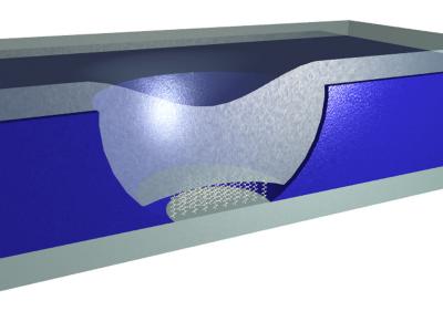
a potentially superior approach for innovative electronics that rely on the spin, and associated magnetic orientation, of electrons. The physicists created a nanoscale test structure to obtain clear evidence of the presence and action of specific molecules and magnetic switching behavior.

Whereas conventional electronic devices depend on the movement of electrons and their charge, spintronics works with changes in magnetic orientation caused by changes in electron spin (imagine electrons as tiny bar magnets whose poles are rotated up and down). Already used in read-heads for computer hard disks, spintronics can offer more desirable properties--higher speeds, smaller size--than conventional electronics. Spintronic devices usually are made of inorganic materials. The use of organic molecules may be preferable, because electron spins can be preserved for longer time periods and distances, and because these molecules can be easily manipulated and self-assembled. However, until now, there has been no experimental confirmation of the presence of molecules in a spintronic structure. The new NIST results are expected to assist in the development of practical molecular spintronic devices.

The experiments, described in the October 9 issue of Applied Physics Letters,* used a specially designed nanoscale "pore" in a silicon wafer. A one-molecule-thick layer of self-assembled molecules containing carbon, hydrogen and sulfur was sandwiched in the pore, between nickel and cobalt electrodes. The researchers applied an electric current to the device and measured the voltage levels produced as electrons "tunneled" through the molecules from the cobalt to the nickel electrodes. (Tunneling, observed only at nanometer and atomic dimensions, occurs when electrons exhibit wave-like properties, which permit them to penetrate barriers.)

The pore structure stabilized and confined the test molecules and enabled good molecule-metal contacts, allowing the scientists to measure accurately temperature-dependent behavior in the current and voltage that confirm electron tunneling through the molecular monolayer. Some electrons can lose energy while tunneling, which corresponds to vibration energies unique to the chemical bonds within the molecules. The NIST team used this information to identify and unambiguously confirm that the assembled molecules remain encapsulated in the pore and are playing a role in the device operation. In addition, by varying the magnetic field applied to the device and measuring the electrical resistance, the researchers identified magnetic switching in the electrodes from matching to opposite polarities. ###

This work was supported in part by the Defense Advanced Research Projects Agency.
Related Posts Plugin for WordPress, Blogger...

Visitors


free counter
Advertise my site free UseAds.com! Add & submit url & exchange text links + increase traffic & improve page rank!

Advertising my web site free online UseAds.com - Add & submit url & exchange text links + increase traffic & promotion marketing website