nanotechnology

Taxol bristle ball: a wrench in the works for cancer

Taxol bristle ball: a wrench in the works for cancer, Dozens of cancer-clogging drug molecules loaded onto tiny gold sphere

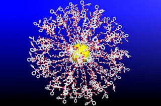
Caption: Using gold nanoparticles, Rice chemists have created tiny spheres that literally bristle with molecules of the anti-cancer drug Taxol. Credit: Eugene Zubarev/Rice University. Usage Restrictions: Must credit.

HOUSTON,  – Rice University chemists have discovered a way to load dozens of molecules of the anti-cancer drug paclitaxel onto tiny gold spheres. The result is a tiny ball, many times smaller than a living cell that literally bristles with the drug.


Paclitaxel, which is sold under the brand name Taxol®, prevents cancer cells from dividing by jamming their inner works.

"Paclitaxel is one of the most effective anti-cancer drugs, and many researchers are exploring how to deliver much more of the drug directly to cancer cells," said lead researcher Eugene Zubarev, the Norman Hackerman-Welch Young Investigator and assistant professor of chemistry at Rice. "We looked for an approach that would clear the major hurdles people have encountered -- solubility, drug efficacy, bioavailability and uniform dispersion -- and our initial results look very promising."

The research is available online and will appear in the Sept. 19 issue of the Journal of the American Chemical Society (J. Am. Chem. Soc. 2007, vol. 129, pgs.11653-11661).

First isolated from the bark of the yew tree in 1967, paclitaxel is one of the most widely prescribed chemotherapy drugs in use today. The drug is used to treat breast, ovarian and other cancers.

Paclitaxel works by attaching itself to structural supports called microtubules, which form the framework inside living cells. In order to divide, cells must break down their internal framework, and paclitaxel stops this process by locking the support into place.

Since cancer cells divide more rapidly than healthy cells, paclitaxel is very effective at slowing the growth of tumors in some patients. However, one problem with using paclitaxel as a general inhibitor of cell division is that it works on all cells, including healthy cells that tend to divide rapidly. This is why patients undergoing chemotherapy sometimes suffer side effects like hair loss and suppressed immune function.

"Ideally, we'd like to deliver more of the drug directly to the cancer cells and reduce the side effects of chemotherapy," Zubarev said. "In addition, we'd like to improve the effectiveness of the drug, perhaps by increasing its ability to stay bound to microtubules within the cell."

Zubarev's new delivery system centers on a tiny ball of gold that's barely wider than a strand of DNA. Finding a chemical process to attach a uniform number of paclitaxel molecules to the ball -- without chemically altering the drugs -- was not easy. Only a specific region of the drug binds with microtubules. This region of the drugs fits neatly into the cell's support structure, like a chemical "key" fitting into a lock. Zubarev and graduate student Jacob Gibson knew they had to find a way to make sure the drug's key was located on the face of each bristle.

Zubarev and Gibson first designed a chemical "wrapper" to shroud the key, protecting it from the chemical reactions they needed to perform to create the ball. Using the wrapped version of the drug, they undertook a series of reactions to attach the drug to linker molecules that were, in turn, attached to the ball. In the final step of the reaction, they dissolved the wrapper, restoring the key.

"We are already working on follow-up studies to determine the potency of the paclitaxel-loaded nanoparticles," Zubarev said. "Since each ball is loaded with a uniform number of drug molecules, we expect it will be relatively easy to compare the effectiveness of the nanoparticles with the effectiveness of generally administered paclitaxel." ###

Research co-authors include Rice graduate student Bishnu Khanal. The research was funded by the National Science Foundation and the Welch Foundation.

Contact: Jade Boyd jadeboyd@rice.edu 713-348-6778 Rice University

Salmon Garnish Points the Way to Green Electronics

A University of Cincinnati (UC) researcher has an unusual approach to developing “green” electronics — salmon sperm.

Professor Andrew Steckl, a leading expert in light-emitting diodes, is intensifying the properties of LEDs by introducing biological materials, specifically salmon DNA.


Ohio Eminent Scholar Andrew Steckl is one of the world's leading experts in photonics. (Photo by Dottie Stover)

Electrons move constantly — think of tiny particles with a negative charge and attention deficit disorder. It is through the movement of these electrons that electric current flows and light is created.


Steckl is an Ohio Eminent Scholar in UC’s Department of Electrical and Computer Engineering. He believed that if the electrons’ mobility could be manipulated, then new properties could be revealed.

In considering materials to introduce to affect the movement of the electrons, Steckl evaluated the source of materials with an eye to supply, especially materials that do not harm the environment.


“Biological materials have many technologically important qualities — electronic, optical, structural, magnetic,” says Steckl. “But certain materials are hard for to duplicate, such as DNA and proteins.” He also wanted a source that was widely available, would not have to be mined, and was not subject to any organization or country’s monopoly. His answer?


Salmon sperm.

“Salmon sperm is considered a waste product of the fishing industry. It’s thrown away by the ton,” says Steckl with a smile. “It’s natural, renewable and perfectly biodegradable.” While Steckl is currently using DNA from salmon, he thinks that other animal or plant sources might be equally useful. And he points out that for the United States, the green device approach takes advantage of something in which we continue to be a world leader — agriculture.

Steckl is pursuing this research in collaboration with the Air Force Research Laboratory. The research was featured recently in such premier scientific publications as the inaugural issue of naturephotonics and on the cover of Applied Physics Letters.


 BioLEDs, devices that incorporate DNA.

“The Air Force had already been working with DNA for other applications when they came to us and said, ‘We know that you know how to make devices,’” quotes Steckl. “They also knew that they had a good source of salmon DNA.” It was a match made in heaven.


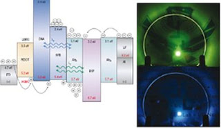
So began Steckl’s work with BioLEDs, devices that incorporate DNA thin films as electron blocking layers. Most of the devices existing today are based on inorganic materials, such as silicon. In the last decade, researchers have been exploring using naturally occurring materials in devices like diodes and transistors.

“The driving force, of course, is cost: cost to the producer, cost to the consumer and cost to the environment” Steckl points out, “but performance has to follow.”

And what a performance — lights, camera, action!


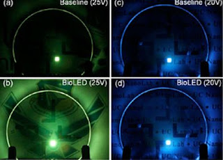
BioLEDs make colors brighter.

“DNA has certain optical properties that make it unique,” Steckl says. “It allows improvements in one to two orders of magnitude in terms of efficiency, light, brightness — because we can trap electrons longer.”


When electrons collide with oppositely charged particles, they produce very tiny packets of light called “photons.”

“Some of the electrons rushing by have a chance to say ‘hello,’ and get that photon out before they pass out,” Steckl explains. “The more electrons we can keep around, the more photons we can generate.” That’s where the DNA comes in, thanks to a bunch of salmon.

“DNA serves as a barrier that affects the motion of the electrons,” says Steckl. It allows Steckl and his fellow researcher, the Air Force’s Dr. James Grote, to control the brightness of the light that comes out.
“The story continues,” says Steckl, again smiling. “I’m receiving salmon sperm from researchers around the world wanting to see if their sperm is good enough.” The next step is to now replace some other materials that go into an LED with biomaterials. The long-term goal is be able to make “green” devices that use only natural, renewable and biodegradable materials.

This research was funded by the United States Air Force.
Here we have the “yin” of biological materials in photonic devices. See Steckl’s “yang” research placing electronics in biological materials: UC Engineering Research Widens Possibilities for Electronic Devices: NSF-funded engineering research on microfluidics at the University of Cincinnati widens the possibilities on the horizon for electronic devices

Contact: Wendy Hart Beckman wendy.beckman@uc.edu 513-556-1826 University of Cincinnati

Researchers improve ability to write and store information on electronic devices

Researchers improve ability to write and store information on electronic devices

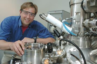
Caption: Matthias Bode, Center for Nanoscale Materials, is shown with his enhanced spin polarized scanning tunneling microscope (SP-STM). His enhanced technique allows scientists to observe the magnetism of single atoms. Use of this method could lead to better magnetic storage devices for computers and other electronics. Credit: DOE/Argonne National Laboratory. Usage Restrictions: None.

New research led by the U.S. Department of Energy's Argonne National Laboratory physicist Matthias Bode provides a more thorough understanding of new mechanisms, which makes it possible to switch a magnetic nanoparticle.


without any magnetic field and may enable computers to more accurately write and store information.

Bode and four colleagues at the University of Hamburg used a special scanning tunneling microscope equipped with a magnetic probe tip to force a spin current through a small magnetic structure. The researchers were able to show that the structure's magnetization direction is not affected by a small current, but can be influenced if the spin current is sufficiently high.

Most computers today use dynamic random access memory, or DRAM, in which each piece of binary digital information, or bit, is stored in an individual capacitor in an integrated circuit. Bode's experiment focused on magneto-resistive random access memory, or MRAM, which stores data in magnetic storage elements consisting of two ferromagnetic layers separated by a thin non-magnetic spacer. While one of the two layers remains polarized in a constant direction, the other layer becomes polarized through the application of an external magnetic field either in the same direction as the top layer (for a "0") or in the opposite direction (for a "1").

Traditionally, MRAM are switched by magnetic fields. As the bit size has shrunk in each successive generation of computers in order to accommodate more memory in the same physical area, however, they have become more and more susceptible to "false writes" or "far-field" effects, Bode said. In this situation, the magnetic field may switch the magnetization not only of the target bit but of its neighbors as well. By using the tip of the Scanning Tunneling Microscope (STM), which has the potential to resolve structures down to a single atom, the scientists were able to eliminate that effect.

Bode and his colleagues were the first ones who did such work with an STM that generates high spatial-resolution data. "If you now push just a current through this bit, there's no current through the next structure over," Bode said. "This is a really local way of writing information."

The high resolution of the STM tip might enable scientists to look for small impurities in the magnetic storage structures and to investigate how they affect the magnet's polarization. This technique could lead to the discovery of a material or a method to make bit switching more efficient. "If you find that one impurity helps to switch the structure, you might be able to intentionally dope the magnet such that it switches at lower currents," Bode said. ###

Contact: Sylvia Carson scarson@anl.gov 630-252-5510 DOE/Argonne National Laboratory

Results of this research were published in the September 14 issue of Science and related research was published earlier this year in Nature.

Funding for this work was provided by Deutsche Forschungsgemeinschaft and the European Union project ASPRINT. This work was conducted prior to Bode's arrival at Argonne. His research at Argonne will be predominately funded by DOE's Office of Basic Energy Sciences.

With employees from more than 60 nations, Argonne National Laboratory brings the world's brightest scientists and engineers together to find exciting and creative new solutions to pressing national problems in science and technology. The nation's first national laboratory, Argonne conducts leading-edge basic and applied scientific research in virtually every scientific discipline.
Argonne researchers work closely with researchers from hundreds of companies, universities, and federal, state and municipal agencies to help them solve their specific problems, advance America 's scientific leadership and prepare the nation for a better future. Argonne is managed by UChicago Argonne, LLC for the U.S. Department of Energy's Office of Science.

'Radio wave cooling' offers new twist on laser cooling

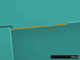
Caption: NIST physicists used radio waves to cool this silicon micro-cantilever, the narrow orange strip across the middle of this colorized micrograph. The cantilever, created by ion etching through a silicon wafer, lies parallel to a silicon radio-frequency electrode. Credit: J. Britton/ NIST. Usage Restrictions: None.

Visible and ultraviolet laser light has been used for years to cool trapped atoms—and more recently larger objects—by reducing the extent of their thermal motion. Now, applying a different form of radiation for a similar purpose, physicists at the National Institute of Standards and Technology (NIST) have used radio waves to dampen the motion of a miniature mechanical oscillator containing more than a quadrillion atoms, a cooling technique that may open a new window into the quantum world using smaller and simpler equipment.

Described in a forthcoming issue of Physical Review Letters,* this demonstration of radio-frequency (RF) cooling of a relatively large object may offer a new tool for exploring the elusive boundary where the familiar rules of the everyday, macroscale world give way to the bizarre quantum behavior seen in the smallest particles of matter and light. There may be technology applications as well: the RF circuit could be made small enough to be incorporated on a chip with tiny oscillators, a focus of intensive research for use in sensors to detect, for example, molecular forces.

The NIST experiments used an RF circuit to cool a 200 x 14 x 1,500 micrometer silicon cantilever—a tiny diving board affixed at one end to a chip and similar to the tuning forks used in quartz crystal watches—vibrating at 7,000 cycles per second, its natural “resonant” frequency. Scientists cooled it from room temperature (about 23 degrees C, or 73 degrees F) to -228 C (-379 F). Other research groups have used optical techniques to chill micro-cantilevers to lower temperatures, but the RF technique may be more practical in some cases, because the equipment is smaller and easier to fabricate and integrate into cryogenic systems. By extending the RF method to higher frequencies at cryogenic temperatures, scientists hope eventually to cool a cantilever to its “ground state” near absolute zero (-273 C or -460 F) , where it would be essentially motionless and quantum behavior should emerge.

Laser cooling is akin to using the kinetic energy of millions of ping-pong balls (particles of light) striking a rolling bowling ball (such as an atom) to slow it down. The RF cooling technique, lead author Kenton Brown says, is more like pushing a child on a swing slightly out of synch with its back-and-forth motion to reduce its arc. In the NIST experiments, the cantilever’s mechanical motion is reduced by the force created between two electrically charged plates, one of which is the cantilever, which store energy like electrical capacitors. In the absence of any movement, the force would be stable, but in this case, it is modulated by the cantilever vibrations. The stored energy takes some time to change in response to the cantilever’s movement, and this delay pushes the cantilever slightly out of synch, damping its motion. ###
* K.R. Brown, J. Britton, R.J. Epstein, J. Chiaverini, D. Leibfried, and D.J. Wineland. 2007. Passive cooling of a micromechanical oscillator with a resonant electric circuit. Physical Review Letters. [Forthcoming].

Novel method for nanostructured polymer thin films

NIST team develops novel method for nanostructured polymer thin films.

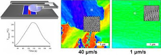
Caption: (Top L.) Schematic of the NIST 'cold zone' annealing process for polymer thin films on a semiconductor wafer. Experiment images are color-coded to show regions with different cylinder orientations, as measured by atomic force microscopy. Relatively rapid transit times (top r.) leave a jumble of different regions that become largely homogeneous at slower speeds (r.). Credit: NIST. Usage Restrictions: None.

All researchers at the National Institute of Standards and Technology (NIST) wanted was a simple, quick method for making thin films of block copolymers or BCPs (chemically distinct polymers linked together) in order to have decent samples for taking measurements important to the microelectronics industry. What they got for their efforts, as detailed in the Sept. 12, 2007, Nano Letters,* was an unexpected bonus: a unique annealing process that may make practical the use of BCP thin films for patterning nanoscale features in next-generation microchips and data storage devices.

BCP thin films have been highly desired by semiconductor manufacturers as patterns for laying down very fine features on microchips, such as arrays of tightly spaced, nanoscale lines. Annealing certain BCP films—a controlled heating process—causes one of the two polymer components to segregate into regular patterns of nanocylinder lines separated by distances as small as five nanometers or equally regular arrays of nanoscale dots. Chemically removing the other polymer leaves the pattern behind as a template for building structures on the microchip.

In traditional oven annealing the quality of the films is still insufficient even after days of annealing. A process called hot zone annealing—where the thin film moves at an extremely slow speed through a heated region that temporarily raises its temperature to a point just above that at which the cylinders become disordered—has previously been used for creating highly ordered BCP thin films with a minimum of defects but little orientation control. For some polymer combinations, the order-disorder transition temperature is so high that it is virtually impossible for manufacturers to heat them sufficiently without degradation occurring.

To eliminate the time and temperature restraints without losing the order yielded by hot zone annealing, the NIST researchers developed a “cold zone” annealing system where the polymers are completely processed well below their order-disorder transition temperature. Properly controlled, the lower-temperature processing not only works with BCPs for which hot-zone annealing is impractical, but, as the NIST experiments showed, also repeatedly produces a highly ordered thin film in a matter of minutes. NIST researchers also discovered that the alignment of the cylinders was controlled by the “cold zone” annealing conditions. Because it is simple, yields consistent product quality and has virtually no limitations on sample dimensions, the NIST method is being evaluated by microelectronic companies to fabricate highly ordered sub 30 nm features.

The next step, the NIST researchers say, is to better understand the fundamental processes that make the cold zone annealing system work so well and refine the measurements needed to evaluate its performance. ###

* B.C. Berry, A.W. Bosse, J.F. Douglas, R.L. Jones and A. Karim.Orientational order in block copolymer films zone annealed below the order-disorder transition temperature. Nano Letters, Vol. 7, No. 9, pp. 2789-2794, (Sept. 12, 2007).

Sheet of carbon atoms acts like a billiard table, physicists find

UC-Riverside research shows graphene, a thin sheet of carbon atoms, has good potential to supplement or replace silicon as an electronic material

RIVERSIDE, Calif. – A game of billiards may never get smaller than this.


Caption: Image shows graphene, which can act as an atomic-scale billiard table, with electric charges acting as billiard balls. Credit: Lau lab, UC-Riverside. Usage Restrictions: None.

Physicists at UC Riverside have demonstrated that graphene – a one-atom thick sheet of carbon atoms arranged in hexagonal rings – can act as an atomic-scale billiard table, with electric charges acting as billiard balls.


The finding underscores graphene’s potential for serving as an excellent electronic material, such as silicon, that can be used to develop new kinds of transistors based on quantum physics. Because they encounter no obstacles, the electrons in graphene roam freely across the sheet of carbon, conducting electric charge with extremely low resistance.

Study results appear in today’s issue of Science.

The research team, led by Chun Ning (Jeanie) Lau, found that the electrons in graphene are reflected back by the only obstacle they meet: graphene’s boundaries.

“These electrons meet no other obstacles and behave like quantum billiard balls,” said Lau, an assistant professor who joined UCR’s Department of Physics and Astronomy in 2004. “They display properties that resemble both particles and waves.”

Lau observed that when the electrons are reflected from one of the boundaries of graphene, the original and reflected components of the electron can interfere with each other, the way outgoing ripples in a pond might interfere with ripples reflected back from the banks.


Caption: Jeanie Lau (left), an assistant professor of physics, seen with Feng Miao (right), her graduate student and first author of the research paper. Credit: Lau lab, UC-Riverside. Usage Restrictions: None.

Her lab detected the “electronic interference” by measuring graphene’s electrical conductivity at extremely low (0.26 Kelvin) temperatures. She explained that at such low temperatures the quantum properties of electrons can be studied more easily.


We found that the electrons in graphene can display wave-like properties, which could lead to interesting applications such as ballistic transistors, which is a new type of transistor, as well as resonant cavities for electrons,” Lau said. She explained that a resonant cavity is a chamber, like a kitchen microwave, in which waves can bounce back and forth.

In their experiments, Lau and her colleagues first peeled off a single sheet of graphene from graphite, a layered structure consisting of rings of six carbon atoms arranged in stacked horizontal sheets. Next, the researchers attached nanoscale electrodes to the graphene sheet, which they then refrigerated in a cooling device. Finally, they measured the electrical conductivity of the graphene sheet.


Caption: Helium-3 refrigerator at UCR that was used by Lau and her research team in the graphene experiments. Credit: Lau lab, UC-Riverside. Usage Restrictions: None.

Graphene, first isolated experimentally less than three years ago, is a two-dimensional honeycomb lattice of carbon atoms, and, structurally, is related to carbon nanotubes (tiny hollow tubes formed by rolling up sheets of graphene)


and buckyballs (hollow carbon molecules that form a closed cage).

Scientifically, it has become a new model system for condensed-matter physics, the branch of physics that deals with the physical properties of solid materials. Graphene enables table-top experimental tests of a number of phenomena in physics involving quantum mechanics and relativity.

Bearing excellent material properties, such as high current-carrying capacity and thermal conductivity, graphene ideally is suited for creating components for semiconductor circuits and computers. Its planar geometry allows the fabrication of electronic devices and the tailoring of a variety of electrical properties. Because it is only one-atom thick, it can potentially be used to make ultra-small devices and further miniaturize electronics. ###

Lau, whose research focuses on nanowires, carbon nanotubes, graphene and other organic molecules, was joined in the research by UCR’s Feng Miao, Sithara Wijeratne, Wenzhong Bao, Yong Zhang and Ulas C. Coskun. The research was performed at UCR. Currently, Zhang is at Southwest University, China; Coskun is at Duke University, N.C.

UCR startup funds and the UCR Center for Nanoscale Science and Engineering supported the research.

The University of California, Riverside is a doctoral research university, a living laboratory for groundbreaking exploration of issues critical to Inland Southern California, the state and communities around the world. Reflecting California's diverse culture, UCR's enrollment of about 17,000 is projected to grow to 21,000 students by 2010.

The campus is planning a medical school and already has reached the heart of the Coachella Valley by way of the UCR Palm Desert Graduate Center. With an annual statewide economic impact of nearly $1 billion, UCR is actively shaping the region's future. To learn more, visit http://www.ucr.edu/ or call (951) UCR-NEWS.

Contact: Iqbal Pittalwala iqbal@ucr.edu 951-827-6050 University of California - Riverside

Computer Memory in Nanoscale Retrieves Data 1,000 Times Faster

Penn Engineers Design Electronic Computer Memory in Nanoscale Form That Retrieves Data 1,000 Times Faster

PHILADELPHIA -- Scientists from the University of Pennsylvania have developed nanowires capable of storing computer data for 100,000 years and retrieving that data a thousand times faster than existing portable memory devices such as Flash memory and micro-drives, all using less power and space than current memory technologies.


Ritesh Agarwal, Assistant Professor, Material Science and Engineering, University of Pennsylvania

Ritesh Agarwal, an assistant professor in the Department of Materials Science and Engineering, and colleagues developed a self-assembling nanowire of germanium antimony telluride, a phase-changing material that switches between amorphous and crystalline structures,

the key to read/write computer memory. Fabrication of the nanoscale devices, roughly 100 atoms in diameter, was performed without conventional lithography, the blunt, top-down manufacturing process that employs strong chemicals and often produces unusable materials with space, size and efficiency limitations.

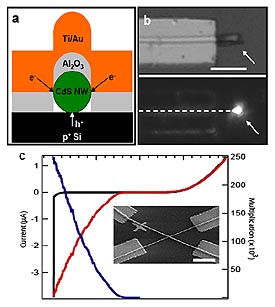
Nanowire electrical injection laser., b, Shows an optical image of a functional laser device described in a, with emission from the end. c. Nanowire Avalanche Photodiode.

Instead, researchers used self-assembly, a process by which chemical reactants crystallize at lower temperatures mediated by nanoscale metal catalysts to spontaneously form nanowires that were 30-50 nanometers in diameter and 10 micrometers in length, and then they fabricated memory devices on silicon substrates.


"We measured the resulting nanowires for write-current amplitude, switching speed between amorphous and crystalline phases, long-term durability and data retention time," Agarwal said.

Tests showed extremely low power consumption for data encoding (0.7mW per bit). They also indicated the data writing, erasing and retrieval (50 nanoseconds) to be 1,000 times faster than conventional Flash memory and indicated the device would not lose data even after approximately 100,000 years of use, all with the potential to realize terabit-level nonvolatile memory device density.

"This new form of memory has the potential to revolutionize the way we share information, transfer data and even download entertainment as consumers," Agarwal said. "This represents a potential sea-change in the way we access and store data."

Phase-change memory in general features faster read/write, better durability and simpler construction compared with other memory technologies such as Flash. The challenge has been to reduce the size of phase change materials by conventional lithographic techniques without damaging their useful properties. Self-assembled phase-change nanowires, as created by Penn researchers, operate with less power and are easier to scale, providing a useful new strategy for ideal memory that provides efficient and durable control of memory several orders of magnitude greater than current technologies.

"The atomic scale of the nanodevices may represent the ultimate size limit in current-induced phase transition systems for non-volatile memory applications," Agarwal said.

Current solid-state technology for products like memory cards, digital cameras and personal data assistants traditionally utilize Flash memory, a non-volatile and durable computer memory that can be erased and reprogrammed electronically. Data on Flash drives provides most battery-powered devices with acceptable levels of durability and moderately fast data access. Yet the technology's limits are apparent. Digital cameras can't snap rapid-fire photos because it takes precious seconds to store the last photo to memory. If the memory device is fast, as in DRAM and SRAM used in computers, then it is volatile; if the plug on a desktop computer is pulled, all recent data entry is lost.

Therefore, a universal memory device is desired that can be scalable, fast, durable and nonvolatile, a difficult set of requirements which have now been demonstrated at Penn.

"Imagine being able to store hundreds of high-resolution movies in a small drive, downloading them and playing them without wasting time on data buffering, or imagine booting your laptop computer in a few seconds as you wouldn't need to transfer the operating system to active memory" Agarwal said.

The research was performed by Agarwal, Se-Ho Lee and Yeonwoong Jung of the Department of Materials Science and Engineering in the School of Engineering and Applied Science at Penn. The findings appear online in the journal Nature Nanotechnology and in the October print edition.
The research was supported by the Materials Research Science and Engineering Center at Penn, the University of Pennsylvania Research Foundation award and a grant from the National Science Foundation.

Contact: Jordan Reese jreese@pobox.upenn.edu 215-573-6604 University of Pennsylvania

Bone-growing nanomaterial could improve orthopaedic implants

Bone-forming cells grow faster and produce more calcium on anodized titanium covered in carbon nanotubes compared with plain anodized titanium and the non-anodized version currently used in orthopaedic implants, new Brown University research shows. The work, published in Nanotechnology, uncovers a new material that can be used to make more successful implants. The research also shows tantalizing promise for an all-new device: a “smart” implant that can sense and report on bone growth.
PROVIDENCE, R.I. [Brown University] — For orthopaedic implants to be successful, bone must meld to the metal that these artificial hips, knees and shoulders are made of. A team of Brown University engineers, led by Thomas Webster, has discovered a new material that could significantly increase this success rate. 


Caption: Anodized titanium covered by carbon nanotubes could lead to a new material for orthopedic implants. Credit: Sirinrath Sirivisoot/Brown University. Usage Restrictions: Must use credit above.


“Possibly a terrific new material”
A titanium surface covereed by carbon nanotubes could lead to faster, better growth of implanted bone-growing cells and an improved success rate for orthopaedic surgery.


The carbon nanotubes could could even self-report, keeping doctors informed about the healing process. Image: Sirinrath Sirivisoot/Brown University


The secret: carbon nanotubes on anodized titanium. The team took titanium – the most popular implant material around – and chemically treated it and applied an electrical current to it. This process, called anodization, creates a pitted coating in the surface of the titanium. Webster and his team packed those pits with a cobalt catalyst and then ran the samples through a chemical process that involved heating them to a scorching 700° C. That caused carbon nanotubes to sprout from each pit.

Researchers then placed human osteoblasts, or bone-forming cells, onto the nanotube-covered samples as well as onto samples of plain and anodized titanium. The samples were placed in an incubator. After three weeks, the team found that the bone cells grew twice as fast on the titanium covered in nanotubes. Cells interacting with the nanotubes also made significantly more calcium – the essential ingredient for healthy bones. Results are published in Nanotechnology.

“What we found is possibly a terrific new material for joint replacement and other implants,” said Webster, associate professor of engineering at Brown. “Right now, bone doesn’t always properly meld to implants. Osteoblasts don’t grow or grow fast enough. Adding carbon nanotubes to anodized titanium appears to encourage that cell growth and function.”

Webster’s long-term vision for the new material is ambitious. With it, Webster hopes to create a new class of implants – ones that can sense bone growth then send that information to an external device. Doctors could monitor the output and determine whether to inject growth hormones or otherwise intervene to avoid additional surgery. Right now, implant patients must get an X-ray or undergo a bone scan to monitor bone growth.

Webster thinks these “biosensing” implants could even be designed to detect infection and be specially coated to release antibiotics or other drugs into the body.

Webster said the biosensing concept would work because when cells make calcium, an electrical current is created. That current can be conducted through carbon nanotubes and transmitted via radio frequency to a handheld device outside the body – a similar process to the one employed by state-of-the-art cardiac pacemakers.

“This technology would be incredibly exciting,” Webster said. “It could significantly improve patient health – and cut down on expensive diagnostic tests and surgery. We still have a long way to go to make an intelligent implant a reality, but our new results are a strong first step.”

Webster’s Brown research team included engineering graduate student Sirinrath Sirivisoot, the lead author of the Nanotechnology article, engineering graduate students Chang Yao and Xingcheng Xiao and professor of engineering Brian Sheldon.
The Coulter Foundation funded the research.

Editors: Brown University has a fiber link television studio available for domestic and international live and taped interviews and maintains an ISDN line for radio interviews. For more information, call the Office of Media Relations at (401) 863-2476. ######

Contact: Wendy Lawton Wendy_Lawton@brown.edu 401-863-1862 Brown University
Related Posts Plugin for WordPress, Blogger...

Visitors


free counter
Advertise my site free UseAds.com! Add & submit url & exchange text links + increase traffic & improve page rank!

Advertising my web site free online UseAds.com - Add & submit url & exchange text links + increase traffic & promotion marketing website